
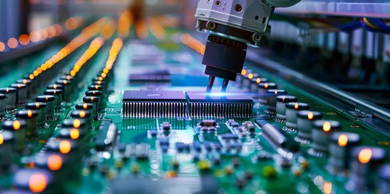
As India positions itself as a global electronics and semiconductor manufacturing hub, the state of Uttar Pradesh is taking decisive steps to lead this transformation. The launch of the Uttar Pradesh Semiconductor Mission (UPSM) is a landmark move aimed at creating an ecosystem that attracts investment, drives innovation, and establishes UP as a key node in the global semiconductor value chain.
What is the UP Semiconductor Mission?
The UP Semiconductor Mission is a government-backed initiative launched to support India’s broader semiconductor vision under the India Semiconductor Mission (ISM). With its focus on policy support, infrastructure development, and talent creation, UPSM aims to:
- Facilitate semiconductor manufacturing, assembly, testing, and packaging (ATMP) units in UP
- Enable fabless design startups, R&D centers, and IP development
- Offer incentives to foreign and domestic investors
- Develop a specialized semiconductor industrial ecosystem in UP
- Partner with global semiconductor companies, research institutions, and local industries
Major Milestone: HCL–Foxconn Semiconductor JV Approved
In May 2025, the Union Cabinet approved a ₹3,706 crore joint venture between HCL Group and Taiwan’s Foxconn, marking a historic leap for the UPSM. The partnership will establish Uttar Pradesh’s first outsourced semiconductor assembly and test (OSAT) facility in the YEIDA region near Jewar Airport.
- The plant will produce 36 million display driver chips per month, catering to sectors like mobiles, laptops, automotive, and medical electronics
- This marks India’s sixth semiconductor unit under the India Semiconductor Mission
- The facility is expected to become operational by 2027
- The project is projected to create over 2,000 direct jobs
This development places Uttar Pradesh on the global semiconductor map, with the state actively contributing to India’s electronics self-reliance.
Strategic Objectives of UPSM
The UP Semiconductor Mission focuses on:
- Attracting Semiconductor Investment
- Developing Infrastructure (e.g., industrial clusters, utilities, logistics)
- Skilling & Talent Development with state-supported institutions
- Public-Private Partnerships (PPPs) for innovation and deployment
- Streamlined Policy Support with fast-track approvals and capital incentives
Why Uttar Pradesh?
Uttar Pradesh offers a compelling mix of:
- Proximity to NCR (Noida–Greater Noida–YEIDA region)
- Access to engineering and technical talent
- Infrastructure readiness with Jewar Airport, expressways, and industrial parks
- A large consumer base and strategic investor policies
The YEIDA region has already been earmarked as a semiconductor and electronics manufacturing hub, with active interest from global and domestic players.
National Alignment: Supporting India’s Semiconductor Vision
UPSM aligns closely with India’s ₹76,000 crore India Semiconductor Mission, and complements national efforts to attract and support chip manufacturers, packaging facilities, and design-led innovation. The recent HCL–Foxconn project showcases how national vision is being executed at the state level with speed and precision.
“Uttar Pradesh is ready to become the silicon heartland of India,” said an official from the YEIDA authority.
Looking Ahead
With this MoU and the growing investor momentum, UPSM is expected to attract more global players, including companies in chip packaging, design, materials, EDA software, and testing tools. Additionally, collaborative efforts are being initiated with academic and skill development partners to create a semiconductor-ready workforce.
Conclusion
The UP Semiconductor Mission is not just a policy initiative — it’s a strategic commitment to make India’s most populous state a global tech manufacturing powerhouse. With visionary leadership, strong public-private partnerships, and landmark collaborations like HCL–Foxconn, Uttar Pradesh is now at the forefront of India's next-generation semiconductor journey.